NANOCOHYBRI will join expertise in characterizing vortex behaviour in different topical superconducting systems, including cuprates, pnictides or MgB2, in nanopatterning pinning centers and in modelling current dynamics in superconductors.
Within WG3, we will explore vortex pinning and current transport in the range of liquid helium temperatures and at high magnetic fields. This remained unaddressed until very recently and is expected to considerably influence new applications. Within this network, we expect interesting synergies between applications and fundamental physics. For instance, the overdoped regime of the cuprates, such as REBa2Cu3O7-x, recently came into focus. Close to the quantum critical point (beyond the optimum Tc), different experiments show a sizeable increase of the pair condensation energy and possible vortex structure maximizing pinning energy. Within NANOCOHYBRI we will provide the combined approach of model, controlled fabrication, visualization at the nanoscale and current carrying tests, needed to engineer artificial pinning centres and obtain the desired critical current enhancement.
At the same time, we will consider manufacturing options that take into account costs, which have to remain affordable. Coated conductors provide a low cost chemical solution and growth. Supported by simulations and visualization of pinning centres and vortex positions, NANOCOHYBRI can considerably help in achieving this goal. Present efforts aim at the range of 20 €/kAm, reducing costs by a factor of five, as compared to the present status. This would enable a fast penetration into the market of machines for energy production or generation of high magnetic fields.
On the other hand, patterned thin films of superconducting materials offer new opportunities to control vortex pinning, obtaining model systems for fundamental studies, providing new devices and improving the properties of sensors based on superconductors.

In low Tc superconductors, advances in patterning allows creating smaller nanowires, unveiling new regimes of conduction, dominated by surface superconductivity and providing enhanced critical field with respect to larger sized wires. 2D patterned arrays provide a unique test-bed for a dynamic transition between a frozen vortex lattice pinned into the array and a moving lattice. The controlled fabrication of large arrays of equally sized pinning centres allows determining precisely critical exponents of vortex transitions through transport experiments (dynamic transitions) and through direct observation using advanced microscopies (order-disorder or pinning induced transitions). In high Tc superconductors, such as YBCO, patterning can take advantage of the strong dependence of its properties on the carrier concentration. We can expect a metal insulator transition by reducing the hole doping. By using a non-homogeneous electric field obtained by nano-engineering the doping level, we can aim at forming reconfigurable pinning potentials. Introducing ferroelectrica in periodic arrays, we can aim at modulating the pinning potential by controlling the electric field on top of the ferroelectrics and modify locally superconducting properties.
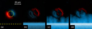
Concerning the methodology, in this WG, we will combine advanced simulation tools, using Ginzburg-Landau functional, electrical characterization to measure the critical current and advanced microscopy tools (such as Scanning Hall magnetometry, scanning SQUID microscopy, including SQUID on a tip microscopy and three-axis vector nanoSQUID, magnetic force microscopy, tunnelling microscopy and optical microscopies) combined with high resolution electron microscopy, to identify defects in the nanoengineered samples and measure positions of single vortices. We will investigate vortex pinning locally by low temperature magneto-optical imaging combined with electrical and heat transport. The Action will also bring new and promising techniques that are still under development to the next level, such as manipulation of individual vortices by injection of quasiparticles and local photon irradiation.
Tasks:
- T 3.1. Investigate vortex pinning energies in the overdoped regime for different nanostructured landscapes.
- T 3.2. Study vortex motion in nanowires and in nanopatterned arrays. T 3.3. Design nanopattern electric field devices into superconductors.