Focused electron beam induced deposition meets materials science
 Authors:
M.Huth, F.Porrati and O.V.Dobrovolskiy
Microelectronic Engineering
Volumes 185–186, 5 January 2018, Pages 9-28
Focused electron beam induced deposition (FEBID) is a direct-write method for the fabrication of nanostructures whose lateral resolution rivals that of advanced electron beam lithography but is in addition capable of creating complex three-dimensional nano-architectures. Over the last decade several new developments in FEBID and focused electron beam induced processing (FEBIP) have led to a growing number of scientific contributions in solid state physics and materials science based on FEBID-specific materials and particular shapes and arrangements of the employed nanostructures.
In this review an attempt is made to give a broad overview of these developments and the resulting contributions in various research fields encompassing mesoscopic physics with nanostructured metals at low temperatures, direct-write of superconductors and nano-granular alloys or intermetallic compounds and their applications, the contributions of FEBID to the field of metamaterials, and the application of FEBID structures for sensing of force or strain, dielectric changes or magnetic stray fields. The very recent development of FEBID towards simulation-assisted growth of complex three-dimensional nano-architectures is also covered. In the review particular emphasis is laid on conceptual clarity in the description of the different developments, which is reflected in the mostly schematic nature of the presented figures, as well as in the recurring final sub-sections for each of the main topics discussing the respective “challenges and perspectives”.
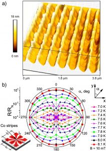
Our group demonstrated for the first time that nanostructures fabricated by FEBID can be used for the extension of the dissipationfree state of superconductors to higher temperatures and larger currents.
