Stoichiometric Bi2Se3 topological insulator ultra-thin films obtained through a new fabrication process for optoelectronic applications
Authors: Matteo Salvato, Mattia Scagliotti, Maurizio De Crescenzi,
Paola Castrucci, Fabio De Matteis, Michele Crivellari, Stefano Pelli Cresi,
Daniele Catone, Thilo Bauch and Floriana Lombardi
Nanoscale, 2020, 12, 12405
Abstract:
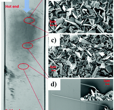
A new fabrication process is developed for growing Bi2Se3 topological insulators in the form of nanowires/nanobelts and ultra-thin films. It consists of two consecutive procedures: first Bi2Se3 nanowires/
nanobelts are deposited by standard catalyst free vapour–solid deposition on different substrates positioned inside a quartz tube. Then, the Bi2Se3, stuck on the inner surface of the quartz tube, is re-evaporated and deposited in the form of ultra-thin films on new substrates at a temperature below 100 °C,
which is of relevance for flexible electronic applications. The method is new, quick, very inexpensive, easy
to control and allows obtaining films with different thickness down to one quintuple layer (QL) during the
same procedure. The composition and the crystal structure of both the nanowires/nanobelts and the thin
films are analysed by different optical, electronic and structural techniques. For the films, scanning tunnelling spectroscopy shows that the Fermi level is positioned in the middle of the energy bandgap as a consequence of the achieved correct stoichiometry. Ultra-thin films, with thickness in the range 1–10 QLs
deposited on n-doped Si substrates, show good rectifying properties suitable for their use as photodetectors in the ultra violet-visible-near infrared wavelength range.
