Within the WG1, the growth and optimization of novel two-dimensional materials and/or interfaces will be done via chemical vapour deposition, ultra high vacuum molecular beam epitaxy or atomic layer deposition. We will fabricate ultimately thin systems—down to a single atomic layer—of deposits on Si. Other two dimensional (2D) materials, such as transition metal dichalcogenides (NbSe2, MoS2, MoSe2, WS2 and WSe2) will be obtained by exfoliation. This procedure is not scalable to wafer sizes but allows obtaining structurally almost ideal materials. The nature of these 2D materials, the characteristic energy and length scales of electron-phonon, spin-orbit and other interactions and correlations are crucial for their potential use in both nanoelectronics and spintronics.
We will also fabricate 2D based nanodevices, ranging from a Hall-Effect bar (HE) structure (with or without gate), a Transmission Line Measurement (TLM) structure, and a Top Gated-Field Effect Transistor (TG-FET) structure. These will be realized either in-situ, by using mechanical masks and capping, and in state-of-the-art clean room facilities equipped with all needed nanofabrication tools. Complex zero-dimensional nanocomposites will be obtained by cluster deposition.
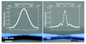
At present we have a considerable control over the properties of disordered superconducting ultrathin films, thanks to which one can cross from a superconductor into an insulator. The insulator as well as the superconductor bear interesting properties that lead to new superconducting behaviour. These address the fundamental problem of electronic correlations in presence of controlled disorder and can be used to improve high frequency applications of superconductors and particle detection.
We will explore extensively electronic properties of these systems using surface sensitive techniques, such as angle-resolved photoemission spectroscopy (ARPES), scanning tunnelling microscopy and spectroscopy (STM/STS) or micro-Raman microscopy, and quantum transport under very high magnetic fields. Ultrafast optical measurements will serve to study anharmonicity and its relation to high critical temperatures. We will explore phonon behaviour in confined systems using X-ray scattering experiments at European Synchrotron radiation facilities and develop new imaging techniques for electronic phase separation phenomena, such as X-ray holography. From the theoretical point of view the superconducting properties of these materials will be studied by Bogoliubov-de Gennes numerical simulations and ab-initio calculations.
Tasks:
- T 1.1. Fabricate, study and model interface superconductors consisting of monolayers, sandwiches, constrictions and materials with a pronounced two-dimensional character.
- T 1.2. Fabricate, study and model hybrid structures combining superconducting with normal, ferromagnetic and semiconducting systems.


