Three-Dimensional Superconducting Nanohelices Grown by He+-Focused-Ion-Beam Direct Writing
Authors:
RETURN TO ISSUEPREVLETTERNEXT
Three-Dimensional Superconducting Nanohelices Grown by He+-Focused-Ion-Beam Direct Writing
Authors: Rosa Córdoba, Dominique Mailly, Roman O. Rezaev, Ekaterina I. Smirnova, Oliver G. Schmid, Vladimir M. Fomin, Uli Zeitler, Isabel Guillamón, Hermann Suderow, José María De Teresa
Nano Lett. 2019, 19, 12, 8597–8604
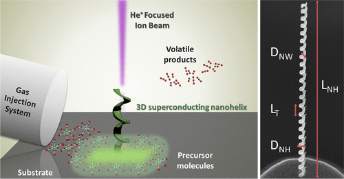
Abstract: Novel schemes based on the design of complex three-dimensional (3D) nanoscale architectures are required for the development of the next generation of advanced electronic components. He+ focused-ion-beam (FIB) microscopy in combination with a precursor gas allows one to fabricate 3D nanostructures with an extreme resolution and a considerably higher aspect ratio than FIB-based methods, such as Ga+ FIB-induced deposition, or other additive manufacturing technologies. In this work, we report the fabrication of 3D tungsten carbide nanohelices with on-demand geometries via controlling key deposition parameters. Our results show the smallest and highest-densely packed nanohelix ever fabricated so far, with dimensions of 100 nm in diameter and aspect ratio up to 65. These nanohelices become superconducting at 7 K and show a large critical magnetic field and critical current density. In addition, given its helical 3D geometry, fingerprints of vortex and phase-slip patterns are experimentally identified and supported by numerical simulations based on the time-dependent Ginzburg–Landau equation. These results can be understood by the helical geometry that induces specific superconducting properties and paves the way for future electronic components, such as sensors, energy storage elements, and nanoantennas, based on 3D compact nanosuperconductors.