“It’s quite challenging to change the functionality of a material”, Anna Palau
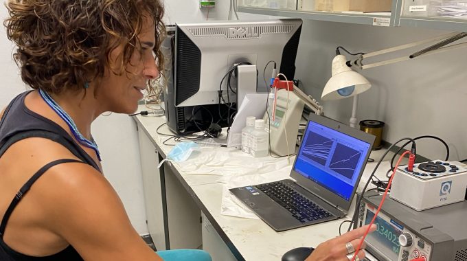
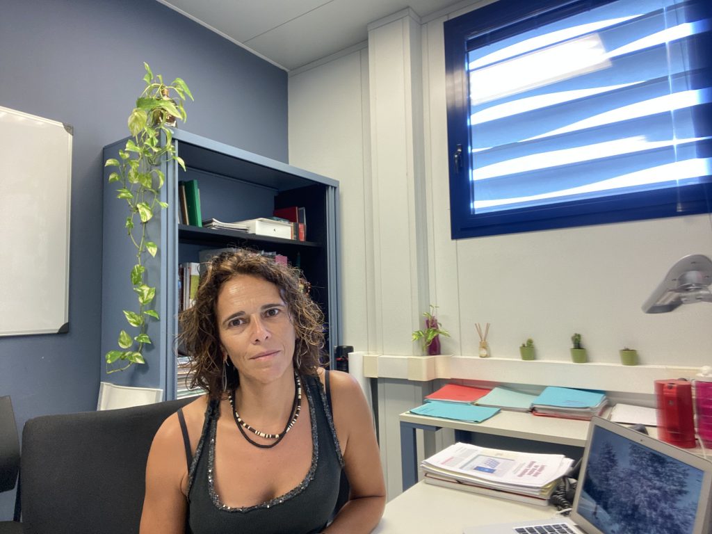
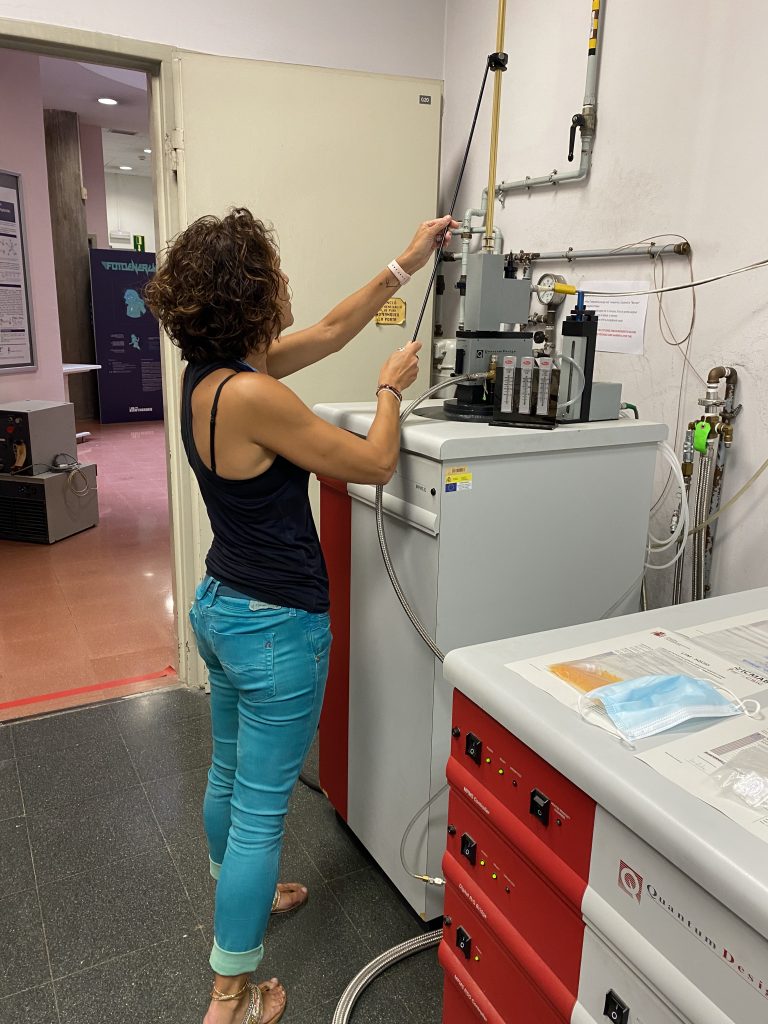
Anna Palau (Spain, 1976) started to work in condensed matter physics to contribute to one of the most recent fields of modern science. During her career, she specialized in oxide materials, in particular high-temperature superconductors. Today, she is a senior scientist at the Institute of Materials Science of Barcelona (ICMAB-CSIC) and has her own group specialized in energy-efficient functional devices based on superconducting, magnetic materials, and hybrid systems.
Q. What are the goals of your research lab?
A. My team research focuses on materials nanoengineering. We try to improve the properties of materials in order to find new functionalities for them, by using different engineering techniques at a very small scale. In our case, for example, we work on complex functional oxide thin films, with versatile physical properties such as magnetism, superconductivity, or switchable resistivity. We combine materials with diverse functionalities, with the purpose of finding novel physical properties or tuning them for the design of high-performance functional devices.
Q. How exactly can you change the material functionalities?
A. Our group tries to work from the material science point of view. We try to tune the material itself at the growing step or modify its properties by using nano-engineering tools. It’s quite challenging to change the functionality of a device by just designing the material properties.
An example would be to combine materials with different physical properties. Depending on what elements you choose and mix, the final performance of the hybrid system can be finely tuned. For example, by combining superconducting and magnetic materials one can obtain hybrid systems really useful to design and create functional devices based on spintronic or fluxonic concepts.
Q. And what would be an example of tuning the base material?
A. In this case, what we can do is to change the composition of the material or its growing conditions of temperature and pressure, among others. In the case of high-temperature superconductors for example, by tuning the amount of oxygen in the structure one can strongly change the electrical properties of the material.
Q. Is there any particular engineering technique that has surprised you more than the others?
A. High-temperature superconductors are materials with a very complex structure, consisting of metal-oxygen layers stack in a variety of sequences. Although a very good planar arrangement is necessary to achieve good properties, one can change and improve the superconducting performance by adding structural defects in the material. This is quite shocking since defects are usually considered to be detrimental to the physical properties and thus it is surprising that defect engineering can bring unforeseen enhancement of functionalities.
Q. Why do you work with high-temperature superconductors? Is there any preference?
A. Low-temperature superconductors have to be cooled down with helium to reach about 5 Kelvin (-268.15ºC). High-temperature superconductors, on the other hand, can work at temperatures as high as 90 Kelvin (-183.15ºC) and can be cooled down with liquid nitrogen. This is a very strong change in the cost because helium is much more expensive than nitrogen. So, if you can work with a device using liquid nitrogen, you can invest what you have saved in improving other areas of your research. Moreover, high-temperature superconductors offer amazing physical behaviors that may not be obtained with conventional low-temperature materials.
Q. What applications can your research have?
A. Our research is in a very fundamental state, but we always try to keep in mind what our materials can be used for. We try to see if the changes we achieve in the materials can solve problems or improve system properties. That is why we are always thinking about the functionality and design of electronic devices, although our research level is in materials engineering, very far from the actual devices in the market.
In any case, we do carry out some projects in collaboration with the industry. For example, we are now working on metamaterials in collaboration with other Nanocohybri scientists, Alejandro Silhanek and Simon Bending. In this project we play with magnetic and superconducting materials, trying to combine them in the right way to guide the magnetic field. The stray electromagnetic field is something that we have around any power cable or any electrical current. Our idea is to use these metamaterials, to concentrate or even harvest the magnetic field and improve the sensitivity of magnetic sensors or actuators, with high potential in the field of the Internet of Things. Thus, we could have autonomous or energy-efficient magnetic sensors with enhanced sensitivity to track and manage information related to public safety, human healthcare, home automation, smart metering, among many others.
Q. Are you working on other collaborative projects?
A. Of course. This is one of the most motivating aspects of our work. We collaborate with other groups in our institution. We have the opportunity to work in a multidisciplinary environment every day with other physicists, chemists, engineers, etc. On the other hand, we always try to collaborate with outside researchers. The Nanocohybri action for example is a very good network to meet other researchers from Europe. Without going any further, I met Alejandro Silhanek at one of the Nanocohybri conferences and we started to collaborate on a project on which we are still working.
Q. What is this collaboration about?
A. This collaboration is based on oxygen migration through electrical fields on complex oxides. The project tries to find a way to design ionic devices, which are devices that are mainly working by changing the position of the ions inside of the material. We are working on this with the electromigration effect, which is based on the oxygen diffusion obtained while applying an electrical current with electrodes connected to the material. When we do this, we are able to move the oxygen atoms inside the material in a controlled way, and thus change its local electrical properties. By doing so, you can generate, for example, binary and multi-state memories or transistors that may be used at the superconducting state or at room temperature.
In this project, our team has the skills and the techniques to grow the material and to design and pattern the devices. Alejandro’s team has the tools and the expertise to induce the electromigration effects and characterize the devices. For example, by collaborating, we designed a system in which we could image the motion of oxygen atoms in superconducting cuprates, with controllable propagation speed. In our lab, we grew the material, patterned it with specially designed geometries and we send the samples to his team. They measured the samples and then we get feedback about how to change the material and patterning to improve the device properties. So, we complement each other very well.
Author: Lucia Torres @osopolita_